O Be Properly Displayed. You Can Send This Data Again
Summary
This commodity explains in detail how to employ and debug SSD1306 displays. In this commodity, I utilize the Segger emWin library and MBEDOS, but for all practical purposes this discussion applies to all other interfaces to the lath including Arduino, Raspberry Pi, Adafruit, etc. I volition say from the outset that I spent far far likewise much time excavation into the inner workings of an 11 year onetime graphics commuter. Oh well, hopefully someone will go some benefit.
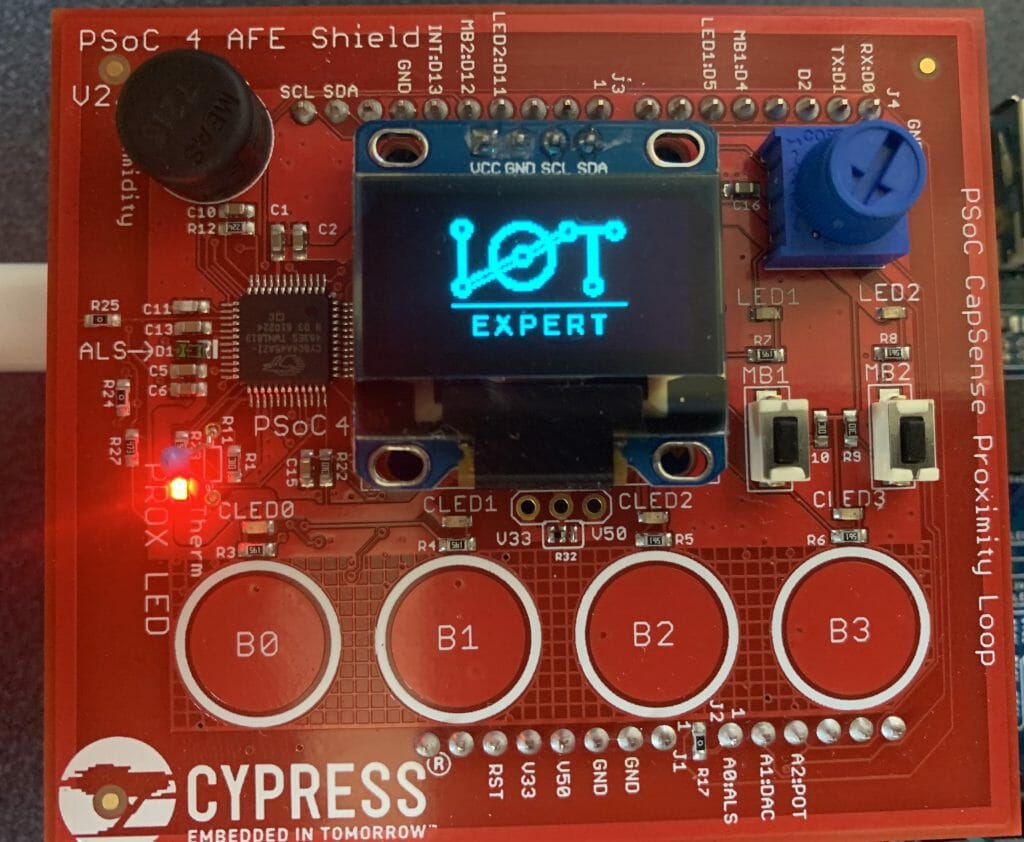
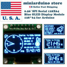
A twelvemonth ago (or so) I designed a user interface board called the CY8CKIT-032 to go with my Cypress WICED WiFi book and class. This board uses a PSoC 4 Analog co-processor which can do a agglomeration of cool stuff. I have a series of articles planned almost that board, but that will be for another twenty-four hours. One of the things that I did was put a 0.96″ I2C OLED Display based on a SSD1306 driver on the board. These displays are widely available from Alibaba and eBay for <$2. I call back that the displays are being used in inexpensive cells phones in Communist china and so at that place are tons of them and they are CHEAP! The bad news is that if you google "ssd1306 issues" you will find an absolute rogues gallery of unpleasantness. It seems that tons of people struggle to get these things working.
This whole thing started concluding week as Cypress released and update to our MBED Os implementation. This update included releasing a consummate set of the Segger emWin drivers. I had been wanting to pace upward to a more robust graphics library than the Adafruit library that I used in this article. I was pleased to meet that our release included the emWin SPAGE commuter which knows how to talk to a bunch of different page based displays including the SSD1306.
Simply, every bit ever, I had to wrestle with the display a little bit before I got everything working. This fourth dimension I wrote down what I did/learned. Then, for this article I volition describe
- The SSD1306 Electrical Interface
- The SSD1306 Software Interface
- The SSD1306 Driver Registers
- The SSD1306 Graphics Data RAM
- Reading from the Frame Buffer
- My Initialization Sequence
- Some Other Initialization Sequences
- A Bunch of Screen Problems & How To Set up
The Electrical Interface
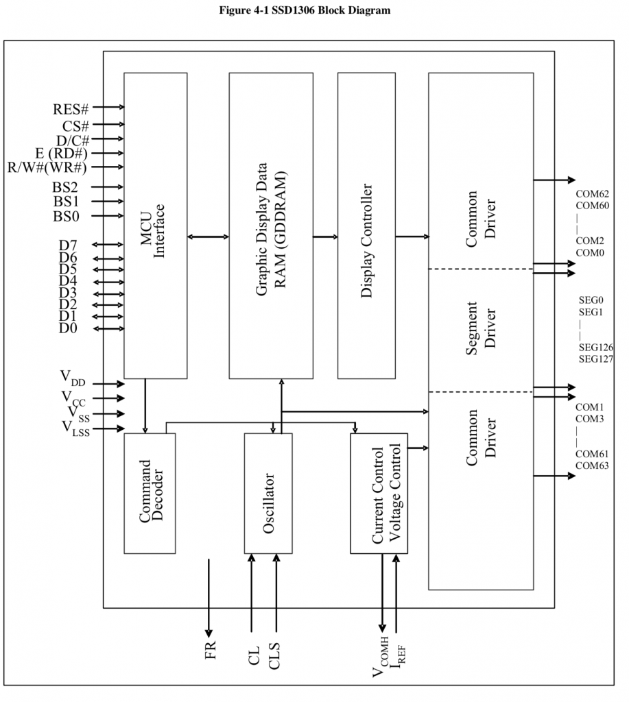
In that location is non a lot to know almost the electrical interface. The information canvass specifies that the device can use I2C, SPI, 6800 and 8080. I accept not seen either the 6800 or 8080 interface put onto any of these OLED displays. Like all driver chips, the SSD1306 has an absolute boatload of pins, in fact, 281. The chip is long and skinny and was made to exist mounted either on the display nether the glass or on the flex connector. Of the 281 pins, 128+64=196 are continued to the segments and commons in the brandish. The residuum of the pins are either capacitors, no-connects, power/ground or data signals. The data signals are
- D0-D7 either parallel data for 8080/6800 or SDA/SCL for I2C or MOSI/MISO for SPI
- Eastward – enable indicate for 6800 or RD for 8080
- R/W# – Read Write for 6800/8080
- CS – Scrap Select for SPI, 8080, 6800
- D/C# – Information or Command for SPI, 6800, 8080 or Slave Accost Select for I2C
- Reset – Bit reset
For the I2C configurations it is common to necktie the reset pin High and non bring the pin to a connector. The SA0 is likewise typically connected via a 0-ohm resistor to either 0 or ane which configures the device to have the seven-bit address 0x3C or 0x3D or 8-scrap 0x78 or 0x7A. Here is a flick of the dorsum of one of my boards where you can see the 0ohm resistor.
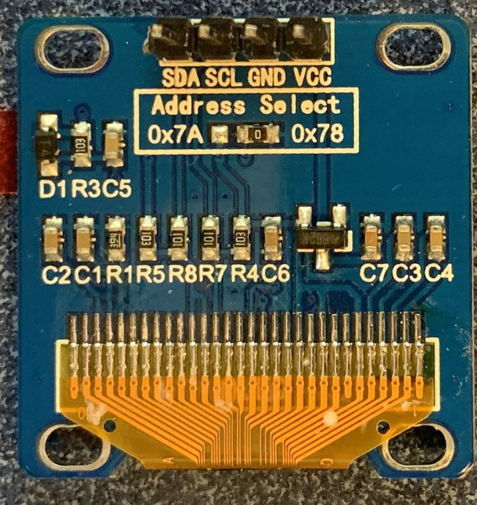
Sometimes all of the data pins are available on the back of the board. This lets you move/add/change the 0-ohm resistors to configure the manner of the chip.
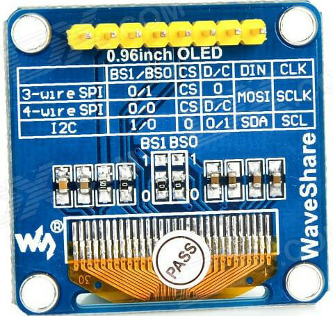
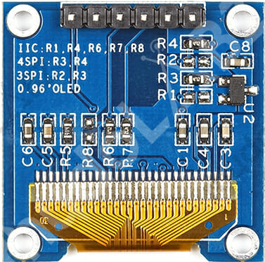
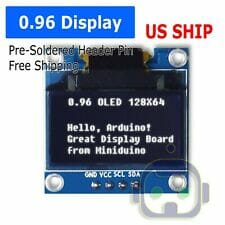
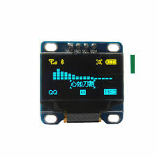
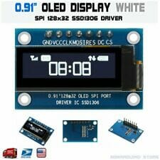
One matter yous should be careful virtually is the I2C connections. I looked effectually on eBay and Alibaba to find a few pictures of the I2C displays. You should observe that all three of these displays are I2C, just all three of them accept a different position and Social club of VCC/GND/SCL/SDL When we ordered displays from China to go onto the CY8CKIT-032 we found displays in the same BATCH that had unlike orders of the VCC/GND.

Here is a SPI version that has reset and data/command pin brought out.
The Software Interface
At that place are two parts to the software interface.
The first part is the control interface. Inside of the chip at that place are a bunch of logic circuits which which configure the accuse pumps, sequence COMs and SEGs, accuse and discharge capacitors etc. All of these things are configurable to allow for different configurations of screens east.g. unlike 10-y sizes, configuration of what wires are connected to what places on the glass etc. Earlier you can get the display to work correctly yous must initialize all of these values past sending commands. All the commands are 1-byte followed past 0 or more control parameters.
The second part is the data interface. Inside of the SSD1306 chip in that location is a Graphics Display DRAM – GDDRAM which has 1 bit for every pixel on the screen. The state machine inside of the bit called the Display Controller volition loop through the bits one by one and display them on the correct place on the screen. This means that your MCU does not need to do anything to keep the display up to date. When y'all want a pixel lit up on the screen y'all just need to write the correct location in the GDDRAM.
For the remainder of this article I volition focus on the serial interface, I2C. How practise you transport commands and data? Simple. When you starting time a transaction you send a control byte which tells the controller what to wait next. There are four legal control bytes.
- 0b10000000 = 0x80 = multiple commands
- 0b00000000 = 0x00 = one command
- 0b11000000 = 0xC0 = multiple data
- 0b01000000 = 0x40 = one data byte
Here is the picture from the datasheet (which I don't find especially illuminating) simply it does describe the control byte.
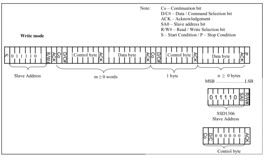
To send commands y'all write to the I2C bus with a control byte, then y'all send the command, then you send the optional parameters. If you want to ship multiple commands you transport the control byte 0x80, the command + parameters as many as you need.
The SSD1306 Commuter Registers
In social club for the driver chip to drive the screen you need to configure:
- How the driver is electrically continued to the OLED Screen
- What are the electrical parameters of the screen
- What are the electrical parameters of the system
- How you desire to address the frame buffer
- The automated gyre configuration settings
- The pixel information for the frame buffer, though it will happily display racket.
If y'all bought this screen from eBay, Adafruit, Alibaba etc. then you will go no say in ane-three, the electric parameters of the organization. Your screen volition come prewired with all of the capacitors, OLED etc already attached to your commuter commons and segments. If you didn't buy the screen prepackaged, then it is highly unlikely you lot are reading this article. What this means is that yous demand to know the initializing sequence required to go the screen to work properly, then you just send the sequence downwards the wire from your MCU to the screen. From looking around on the internet, information technology appears to me that there in only one parameter that is different in any of the screens that I could find. Specifically the number of lines on the screen – either 32 or 64. Which means that all of these initialization implementations should actually on accept one divergence register 0xA8 should be set to either n-i aka 31 or 63
The other difference that you will see betwixt different implementations is the retentivity address mode. In other words, how do you want to write information into the frame buffer from the MCU. Many of the open up source graphics libraries use "Horizontal" mode. The Segger emWin library that I am using uses "Folio" mode. More on this later.
When you look in the data sheet, unfortunately they mix and match the order of the data. Even so, from the information canvas, the categories are:
- Fundamental Commands
- Scrolling Commands
- Address Setting Commands
- Hardware Configuration
- Timing and Driving Scheme
- Charge Pump
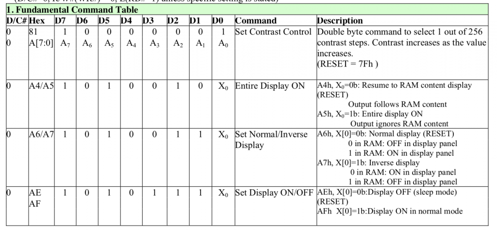
I won't put screen shots of the whole information sheet into this article, just I will show the command table and make a few clarifications on the text. Or at to the lowest degree I will clarify places where I got dislocated.
Every bit to the fundamental commands. I tried a bunch of different dissimilarity settings on my screens and could non tell the difference betwixt them. I tried from 0x10 to 0xFF and they all looked the aforementioned to me. The best course of action is to use the default 0x7F. I don't really know why there is a command 0xA5 "Entire Display ON ignore RAM". The data sheet says "A5h control forces the entire display to be "ON", regardless of the contents of the display data RAM". I can't think of a unmarried apply instance for this. I suppose that if you issue 0xAE the screen volition exist all blackness… and if you lot effect 0xA5 the screen will be all white? Simply why?
And my definitions in the C commuter file:
//////////////////////////////////////////////////////////////////////// // Fundamental Command Table Page 28 //////////////////////////////////////////////////////////////////////// #ascertain OLED_SETCONTRAST 0x81 // 0x81 + 0-0xFF Contrast ... reset = 0x7F // A4/A5 commands to resume displaying data // A4 = Resume to RAM content display // A5 = Ignore RAM content (but why?) #define OLED_DISPLAYALLONRESUME 0xA4 #define OLED_DISPLAYALLONIGNORE 0xA5 // 0xA6/A7 Normal 1=white 0=black Inverse 0=white 1=black #define OLED_DISPLAYNORMAL 0xA6 #define OLED_DISPLAYINVERT 0xA7 // 0xAE/AF are a pair to turn screen off/on #define OLED_DISPLAYOFF 0xAE #ascertain OLED_DISPLAYON 0xAF
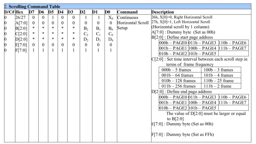
In the next department of the command table are the "Scrolling" commands. Information technology appears that this graphics chip was setup to display text that is 8-pixels loftier. The scrolling commands will let you move the screen upwardly/downward and left/right to curlicue automatically without having to update the the frame buffer. In other words information technology can efficiently curlicue the screen without a bunch of load on your MCU CPU or on the data bus betwixt them. The Adafruit graphics library provides the scrolling commands. However, I am not using them with the Segger Library.
The next section has the commands to configure how your MCU writes data into the Graphics RAM aka the frame buffer. These commands autumn into two categories. Showtime the address mode. The accost modes help you efficiently write the GDDRAM. When yous send information to the frame buffer you really don't want to send
- address, pixel, accost, pixel, …
What you really would like to practice is transport
- Address, pixel, pixel, pixel … (and have the address be automatically incremented
At get-go blush you might retrieve… why do I need a mode? Well there are some people who desire the 10 address incremented… there are some people who want the y-address incremented and there are some people who want to have page address access. And what do you practise when you lot get to the cease of a line? or a column or a page? and what does the end hateful?
The second set of commands in this table are the commands to fix the starting address before yous write data.
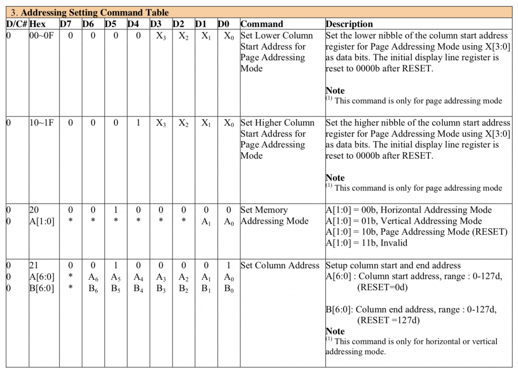
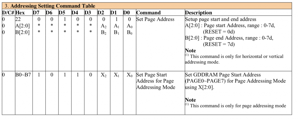
//////////////////////////////////////////////////////////////////////// // Accost Setting Command Table //////////////////////////////////////////////////////////////////////// // 00-0F - set lower nibble of page address // 10-1F - set upper niddle of page address #define OLED_SETMEMORYMODE 0x20 #define OLED_SETMEMORYMODE_HORIZONTAL 0x00 #define OLED_SETMEMORYMODE_VERTICAL 0x01 #define OLED_SETMEMORYMODE_PAGE 0x02 // 0x20 + 00 = horizontal, 01 = vertical 2= page >=3=illegal // Only used for horizonal and vertical address modes #ascertain OLED_SETCOLUMNADDR 0x21 // two byte Parameter // 0-127 column commencement accost // 0-127 column end address #define OLED_SETPAGEADDR 0x22 // 2 byte parameter // 0-seven page first address // 0-7 page end Address // 0xB0 -0xB7 ..... Pick folio 0-vii
The hardware configuration registers let the LED display maker to hookup the common and segment signals in an order that makes sense for the placement of the chip on the OLED drinking glass. For a 128×64 display there are at least 196 wires, so the routing of these wires may be a total hurting in the ass depending on the location of the bit. For instance the left and right might be swapped… or half the wires might come out on one side and the other half on the other side. These registers allow the lath designer flexibility in making these connections. Commands 0xA0, 0xA1, 0xA8, 0xC0, 0xC8, 0xD3, 0xDa will all be fixed based on the layout. Yous take no control and they need to exist fix correctly or something crazy will come out.
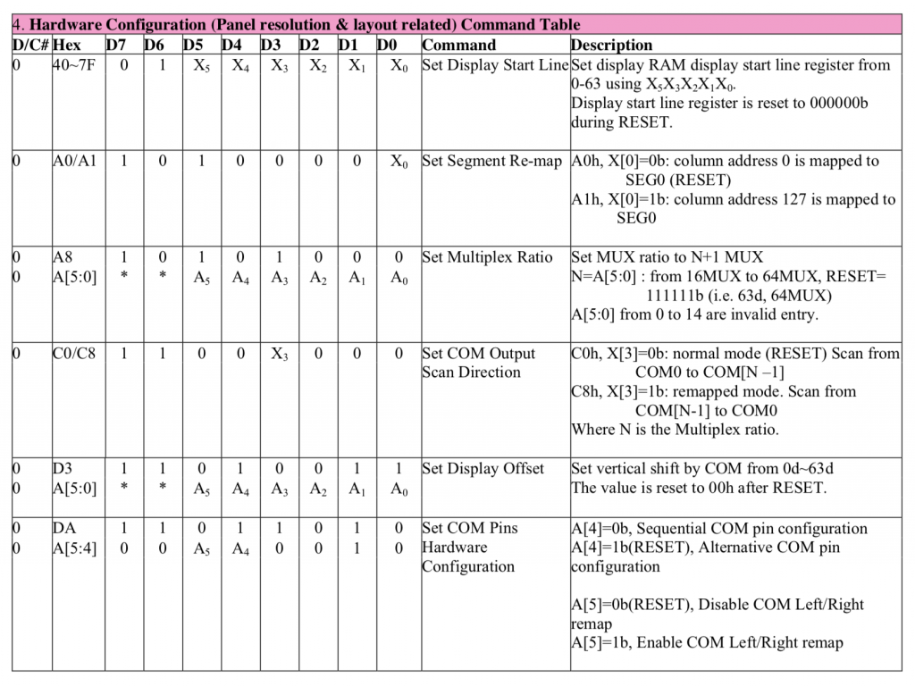
//////////////////////////////////////////////////////////////////////// // Hardware Configuration //////////////////////////////////////////////////////////////////////// // 40-7F - ready address startline from 0-127 (6-$.25) #define OLED_SETSTARTLINE_ZERO 0x40 // Y Management #define OLED_SEGREMAPNORMAL 0xA0 #ascertain OLED_SEGREMAPINV 0xA1 #define OLED_SETMULTIPLEX 0xA8 // 0xA8, number of rows -1 ... e.yard. 0xA8, 63 // X Direction #define OLED_COMSCANINC 0xC0 #define OLED_COMSCANDEC 0xC8 // double byte with image wrap ...probably should exist 0 #define OLED_SETDISPLAYOFFSET 0xD3 // Double Byte Hardware com pins configuration #define OLED_SETCOMPINS 0xDA // legal values 0x02, 0x12, 0x022, 0x032
The next sections of commands are role of the electrical configuration for the glass.
0xD5 substantially sets up the display update rate by ane) setting the brandish update clock frequency and 2) setting up a divider for that clock.
0xDB and 0xD9 sets up a parameter that is brandish dependent. That being said I tried a bunch of unlike values and they all wait the same to me.
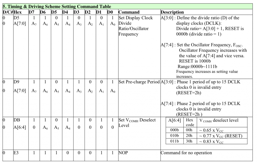
//////////////////////////////////////////////////////////////////////// // Timing and Driving Scheme Settings //////////////////////////////////////////////////////////////////////// #define OLED_SETDISPLAYCLOCKDIV 0xD5 #define OLED_SETPRECHARGE 0xD9 #define OLED_SETVCOMDESELECT 0xDB #ascertain OLED_NOP 0xE3
These displays crave a loftier voltage to plan the liquid crystal in the display. That voltage can either exist supplied by an external pin or by an internal charge pump. All the displays that I take seen use an internal charge pump.
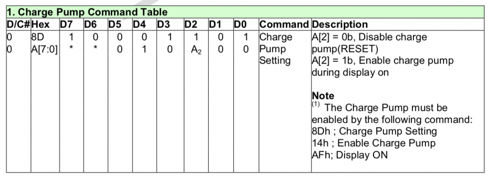
//////////////////////////////////////////////////////////////////////// // Charge Pump Regulator //////////////////////////////////////////////////////////////////////// #define OLED_CHARGEPUMP 0x8D #define OLED_CHARGEPUMP_ON 0x14 #ascertain OLED_CHARGEPUMP_OFF 0x10
The SSD1306 Graphics Data RAM
In order to really become information to display on the screen you lot need to write 1's and 0's into the Graphics Data RAM that represents your epitome. The retention is actually organized into viii pages that are each 128 $.25 wide and eight bits tall. This means that if yous write 0b10101010 to location (0,0) you will become the outset eight pixels in a column on the screen to be on,off,on,off,on,off,on,off. Find that I said vertical column and non row. Here is a movie from the data sheet. That shows the pages:
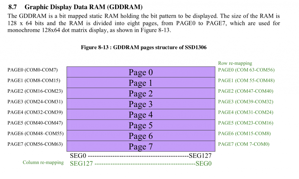
So they show you in the information sheet that the pixels go down from the offset row of the folio.
In order to brand the writing procedure easier and lower bandwidth the SSD1306 has 3 automated addressing modes.
- Horizontal – Set the page address commencement, end and the cavalcade beginning and end… bytes write 8 vertical pixels on the page. Each byte write advances the column until it wraps to the next page and resets the column to the "start"
- Vertical – Gear up the page address start, end and the column starting time and end… bytes write eight vertical pixels on the page. Each byte write advances the page until it wraps vertically where it increments the cavalcade and resets the page back to the start page.
- Page – Set the page address and column commencement/end. Each byte writes vertically. Wraps dorsum onto the same page when it hits the cease column.
In Horizontal and Vertical style you
- Set the range of columns that y'all want to write (using 0x22)
- Set the range of pages you want to write (using 0x21)
- Write bytes
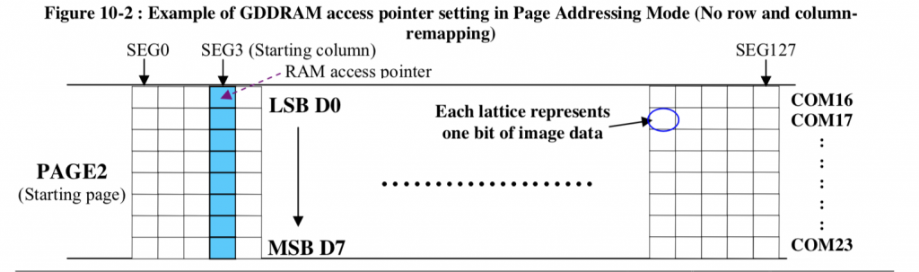
In the folio style you
- Gear up the folio (remember you tin only write ane page at a time in folio manner) using 0xB0-0xB7
- Gear up the start column using 0x0? and 0x1?
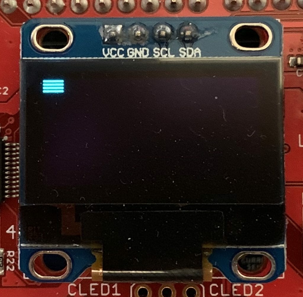
Here is a film from the data sheet of horizontal address style:
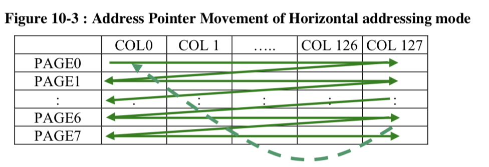
In this flake of case lawmaking I am saying to iterate through the pages 0->7… in other words all of the pages. And to start in column 0. This example will make 12 columns of pixels each eight high starting a (0,0) on the screen…
char horizontalExample[]= { 0xAE, 0x20, /// accost mode 0x00, // Horizontal 0xA4, 0xAF, 0x22, //Gear up page address range 0, vii, 0x21, // cavalcade start and end address 0, 127, }; I2C_WriteCmdStream(horizontalExample, sizeof(horizontalExample)); // Write twelve bytes onto screen with 0b10101010 for(int i=0;i<12;i++) I2C_WriteData(0xAA); Here is a picture of what it does.
Here is a picture from the data canvass of vertical address mode:
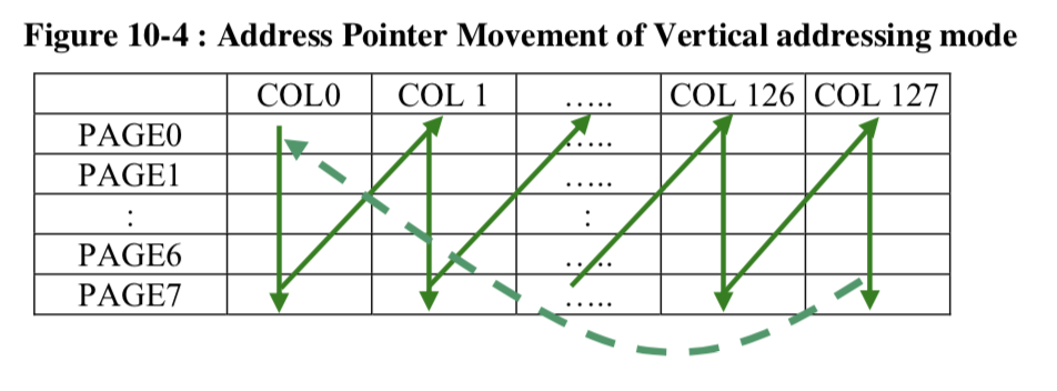
This example lawmaking sets the page range to 0–>7 (the whole screen) and the cavalcade range 0–>127 (the whole screen). Then writes 12 bytes. You can run into it wrap at the bottom and move back to folio 0 cavalcade i.
char verticalExample[]= { 0xAE, 0x20, /// address mode 0x01, // vertical 0xA4, 0xAF, 0x22, //Set page address range 0, seven, 0x21, // column first and end accost 0, 127, }; I2C_WriteCmdStream(verticalExample, sizeof(verticalExample)); // Write twelve bytes onto screen with 0b10101010 for(int i=0;i<12;i++) I2C_WriteData(0xAA); 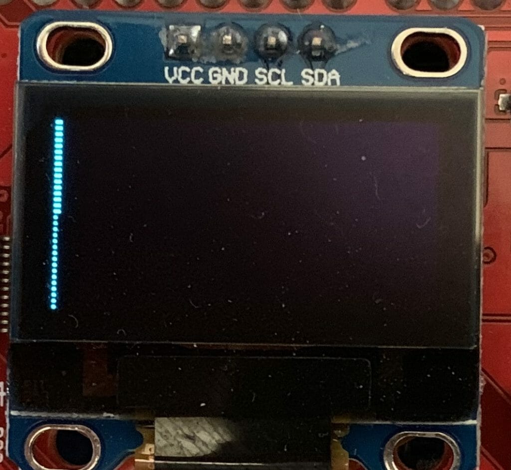
In folio mode you lot just gear up the folio and the offset and cease column. 0xB0 means page 0, 0xB1 means page 1… 0xB7 means folio 7.
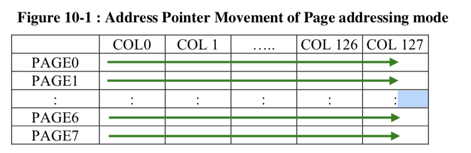
You can see that I started from column 0x78 (meaning cavalcade 120) and that it wraps back to column 0 on the SAME page.
char pageExample[]= { 0xAE, 0x20, // accost way 0x02, // Page way 0xA4, // Resume from ram 0xAF, // Screen on 0xB0, // Start from page 0 // Start from column 0x78 aka 120 0x08, // Column lower nibble address 0x17 // Cavalcade upper crumb accost }; I2C_WriteCmdStream(pageExample, sizeof(pageExample)); // Write twelve bytes onto screen with 0b10101010 for(int i=0;i<12;i++) I2C_WriteData(0xAA); Here is what it looks similar.
Reading from the Frame Buffer
Now that you know how to write to the Frame Buffer, the side by side question is how exercise you lot read? For case if you want to plow on 1 pixel (of a byte) but get out the others solitary can you do this? The answer is NO. In serial mode the device only writes. In all of the Graphics libraries that I take seen they handle this by having a Frame Buffer in the MCU equally well. Duplicated resources… oh well.
My Initialization Sequence
I accept a role that writes an assortment of bytes to the command registers. So for me to initialize the screen I just need to set that array. Here is my best known setup.
const char initializeCmds[]={ //////// Fundamental Commands OLED_DISPLAYOFF, // 0xAE Screen Off OLED_SETCONTRAST, // 0x81 Set contrast control 0x7F, // 0-FF ... default half style OLED_DISPLAYNORMAL, // 0xA6, //Set normal display //////// Scrolling Commands OLED_DEACTIVATE_SCROLL, // Deactive scroll //////// Addressing Commands OLED_SETMEMORYMODE, // 0x20, //Set retentiveness address mode OLED_SETMEMORYMODE_PAGE, // Folio //////// Hardware Configuration Commands OLED_SEGREMAPINV, // 0xA1, //Set segment re-map OLED_SETMULTIPLEX, // 0xA8 Fix multiplex ratio 0x3F, // Vertical Size - one OLED_COMSCANDEC, // 0xC0 Set COM output scan management OLED_SETDISPLAYOFFSET, // 0xD3 Gear up Display Outset 0x00, // OLED_SETCOMPINS, // 0xDA Fix COM pins hardware configuration 0x12, // Alternate com config & disable com left/right //////// Timing and Driving Settings OLED_SETDISPLAYCLOCKDIV, // 0xD5 Prepare display oscillator frequency 0-0xF /clock divide ratio 0-0xF 0x80, // Default value OLED_SETPRECHARGE, // 0xD9 Set pre-changed menses 0x22, // Default 0x22 OLED_SETVCOMDESELECT, // 0xDB, //Ready VCOMH Deselected level 0x20, // Default //////// Charge pump regulator OLED_CHARGEPUMP, // 0x8D Set accuse pump OLED_CHARGEPUMP_ON, // 0x14 VCC generated by internal DC/DC circuit // Turn the screen back on... OLED_DISPLAYALLONRESUME, // 0xA4, //Ready entire display on/off OLED_DISPLAYON, // 0xAF //Prepare brandish on }; Some other Initialization Sequences
If you lot look around you will detect many unlike SSD1306 libraries. You lot can run this search on github.
Here is one instance from https://github.com/vadzimyatskevich/SSD1306/blob/master/src/ssd1306.c This is pretty much the same as mine except that the author put them in some other order than the data sheet. I am non a huge fan of "ssd1306Command( SSD1306_SEGREMAP | 0x1)" but it does work.
void ssd1306Init(uint8_t vccstate) { _font = (FONT_INFO*)&ubuntuMono_24ptFontInfo; // Initialisation sequence ssd1306TurnOff(); // 1. set mux ratio ssd1306Command( SSD1306_SETMULTIPLEX ); ssd1306Command( 0x3F ); // ii. fix display offset ssd1306Command( SSD1306_SETDISPLAYOFFSET ); ssd1306Command( 0x0 ); // 3. set display first line ssd1306Command( SSD1306_SETSTARTLINE | 0x0 ); ssd1306Command( SSD1306_MEMORYMODE); // 0x20 ssd1306Command( 0x00); // 0x0 human activity like ks0108 // four. ready Segment re-map A0h/A1h ssd1306Command( SSD1306_SEGREMAP | 0x1); // 5. Set up COM Output Scan Management C0h/C8h ssd1306Command( SSD1306_COMSCANDEC); // six. Set COM Pins hardware configuration DAh, 12 ssd1306Command( SSD1306_SETCOMPINS); ssd1306Command( 0x12); // 7. Set Contrast Command 81h, 7Fh ssd1306Command( SSD1306_SETCONTRAST ); if (vccstate == SSD1306_EXTERNALVCC) { ssd1306Command( 0x9F ); } else { ssd1306Command( 0xff ); } // 8. Disable Entire Display On A4h ssd1306Command( SSD1306_DISPLAYALLON_RESUME); // 9. Set Normal Brandish A6h ssd1306Command( SSD1306_NORMALDISPLAY); // 10. Gear up Osc Frequency D5h, 80h ssd1306Command( SSD1306_SETDISPLAYCLOCKDIV); ssd1306Command( 0x80); // eleven. Enable charge pump regulator 8Dh, 14h ssd1306Command( SSD1306_CHARGEPUMP ); if (vccstate == SSD1306_EXTERNALVCC) { ssd1306Command( 0x10); } else { ssd1306Command( 0x14); } // 12. Brandish On AFh ssd1306TurnOn(); } Here is some other example from git@github.com:lexus2k/ssd1306.git
https://github.com/lexus2k/ssd1306/blob/principal/src/lcd/oled_ssd1306.c
Honestly if I had plant this originally I would not have gone to all the trouble.
static const uint8_t PROGMEM s_oled128x64_initData[] = { #ifdef SDL_EMULATION SDL_LCD_SSD1306, 0x00,
0 Response to "O Be Properly Displayed. You Can Send This Data Again"
Postar um comentário